TPU (v1): Jack of none, Master of one
The TPU Thesis: Google’s Power Play in the AI Arena
In today’s world, AI tools and their integration into our daily lives have sparked a surge in computational demands at data centers. One at a time, everything around us will be rewritten by AI. While there’s a case to be made for edge AI, most compute today happens in vast data centers.
At the heart of these data centers, GPUs (Graphics Processing Units) reign supreme as the primary computational workhorses powering these AI-driven workloads. The data center GPU market share in 2023 is est to be $13.1 bil and is expected to grow to $120.5 bil in 2032. Nvidia currently commands a staggering 92% market share in data center GPUs.
Major cloud service providers like AWS, Azure and Google cloud are experiencing increase in ML workloads. Most cloud providers rely heavily on Nvidia for their supply of GPUs. But Google, unlike the others, anticipated this as early as 2006. The need to build an Application Specific Integrated Circuit (ASIC) to account for the fast growing compute demands of neural networks - you see Google was all in on AI very early on - became urgent in 2013.
Enter the Tensor Processing Unit (TPU). Google just announced its 6th generation of TPUs (trillium), but its important for us to understand how it all started, the design philosophy of this chip and why it’s integral to Google’s edge in AI (pun fully intended) - full vertical integration!
TPU v1’s Dawn
The dire need for a custom chip to handle deep learning workloads, that were already deployed in production in Google products at the time, forced Google to design, verify, build and deploy the chip in its data centers in just 15 months, a process that usually takes several years. Norm Jouppi, one of the principal architects of the MIPS processor, was the tech lead on this project. He remarked, “we were hiring the team as we were building the chip.”
At the time, the TPU delivered 15-30x higher performance and 30-80x higher performance-per-watt than comtemprary CPUs and GPUs.
The TPU v1’s Unconventional Blueprint: Where metal met math
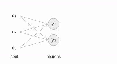
To understand why TPUs were designed the way they were, it’s important to have an understand of mathematical operations that undefly neural networks (or ChatGPT for those new to the scene smh).
Each neuron in a neural net (don’t worry about understanding exactly) does the following calculations:
- Multiply: input data (x) with weights (w)
- Add: intermediary results to aggregate the neuron’s state
- Activation function (f): this brings essential non-linearity in an otherwise linear operation of (1.) and (2.)
Neural nets have to operate over millions (today billions) of such values, amounting to massive compute. For their first optimization, rather than operating on bigger 32-bit or 16-bit float (decimal values) operations, the team decided to operate on 8-bit integers instead. Their blog has a great analogy here. This technique is called quanitization, an optimization that uses 8-bit integers to approximate an arbitrary value between a predetermined min and max value.
Quanitization mapping
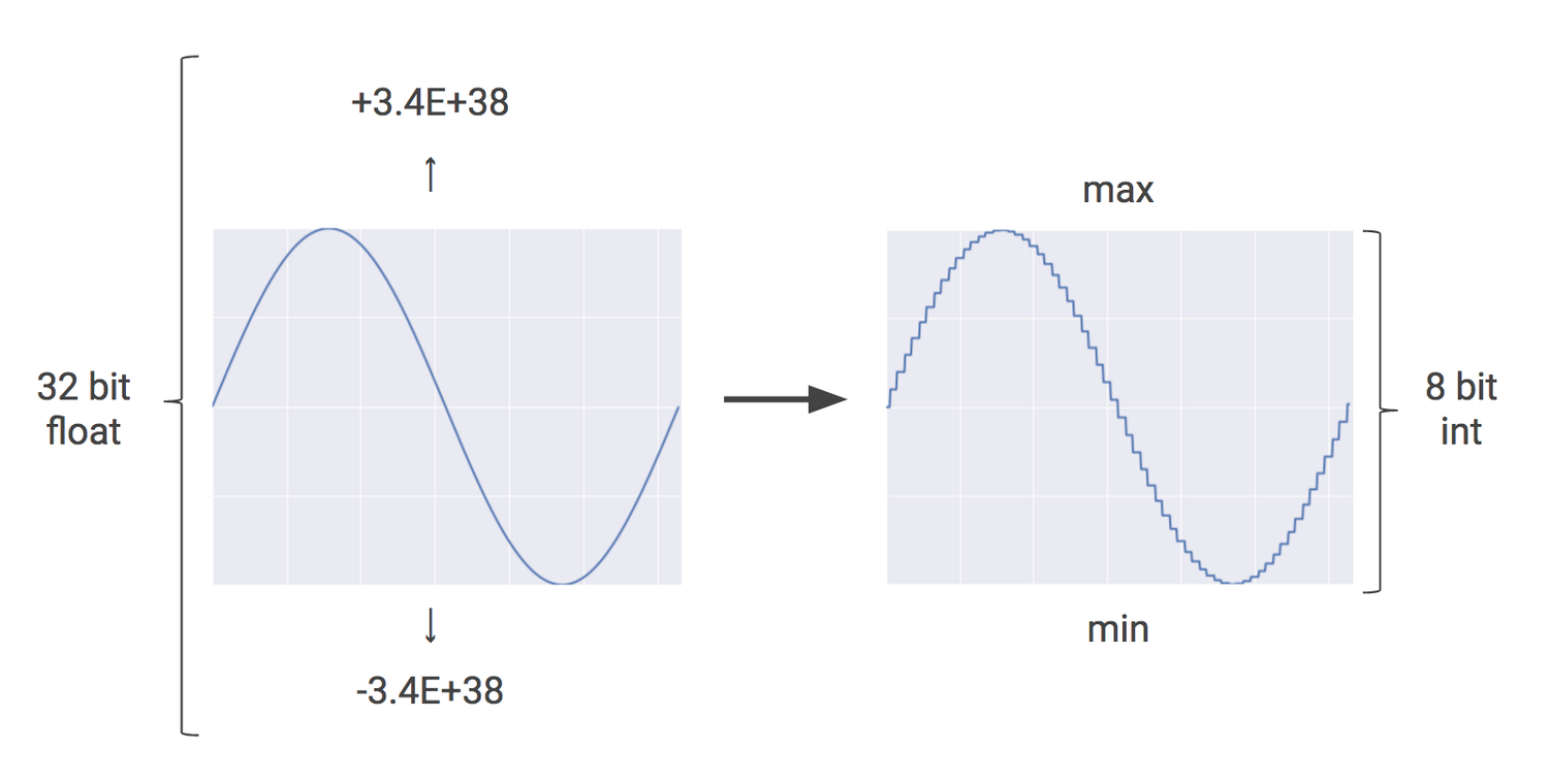
This integer approximation of float values reduced the hardware footprint and energy consumption. The TPU contained 65,536 8-bit integer multipliers, while the GPUs used widely at the time contained a few thousand 32-bit float multipliers.
The TPU included the following essential components:
- Matrix Multiplier Unit (MXU): 65,536 8-bit multiply-add unit for matrix operations.
- Unified Buffer (UB): 24MB of SRAM working as registers.
- Activation Unit (AU): Hardwired activation functions.
They chose a Complex Instruction Set Computer (CISC) style for the TPUs instruction set to run commands.
Google designed the MXU to process hundreds of thousands of operations in a single clock cycle. How? A systolic array.
CPUs were designed to be general purpose chips, which involves storing values in registers and telling the arithmetic-logic units which registers to read values from and operate on. This generality and variety of processing ability comes at a cost in terms of chip area and power consumption.
In an MXU, however, the matrix multiplication operation reuses both inputs and weights many times to produce the output. So each input value can be read once without storing it back in a register. Only spacially adjacent ALUs are connected, making it short and energy efficient. Addition and multiplication is performed in fixed patterns. It’s called systolic because the data flows through the chip in waves, like a heart pumping blood.
Systolic array input vector by weight matrix multiplication
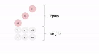
The TPUs MXU systolic array contains 256x256 = 65,536 ALUs. That’s 65,536 8-bit multiply-adds every clock cycle. Since the TPU ran at 700 MHz (700 x 10^6 clock cycles per second) it could run 46 x 10^12 multiple-adds every second or 92 Teraops per second. Mind blowing! In contrast, the CPU could do a few operations per cycle (not second), GPU could do tens of thousands and the TPU hundreds of thousands.
The TPU Legacy: A Glimpse into the Future of AI Acceleration
Today, Google has announced their 6th generation of trillium TPU v6 chips. This custom silicon, among other things, gives Google an edge above other players in AI. They’re clearly not as dependent on Nvidia GPUs as are other companies. Google’s latest Gemini models are completely trained on their own TPUs.
In later articles, I’ll dive deeper into developments across subsequent version of the TPU leading to the latest. The TPU is Google’s edge in AI.
Sources
An in-depth look at Google’s first Tensor Processing Unit (TPU)
Quantifying the performance of the TPU, our first machine learning chip
In-Datacenter Performance Analysis of a Tensor Processing Unit TM
Announcing Trillium, the sixth generation of Google Cloud TPU
PS
I’m only human, a biological language model (maybe little better than that I can give myself more credit), and I may make mistakes in my research. Open to feedback in the issues section of this blog repository.